Front Page Header

| Temporary Bonding & Debonding | Wafer Support System (3M Solution)
| Temporary Debonding
|
|---|---|---|
| Wafer Reclaim Service |
| |
| Polar/ Single | Cleaning
| Etching
Solvent
|
| Wet Bench | Cleaning
Plating
| Solvent Tool
Etching
|
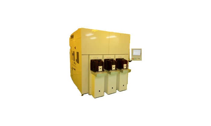
Temporary bonding and debonding are essential processes in semiconductor manufacturing. This technology involves temporarily bonding a device wafer to a carrier wafer using an intermediate material, which provides physical stability for thin wafers or wafers to be trimmed during processing. This allows the delicate device wafer to be processed with additional mechanical support. The wafer and carrier are debonded once the necessary processing steps are completed. In this tool, the wafer and carrier are bonded with adhesive through UV curing and debonded via IR laser at room temperature. These processes enable efficient handling and processing of wafers in semiconductor manufacturing.
Process | Application | Advantage |
|---|---|---|
|
|
|
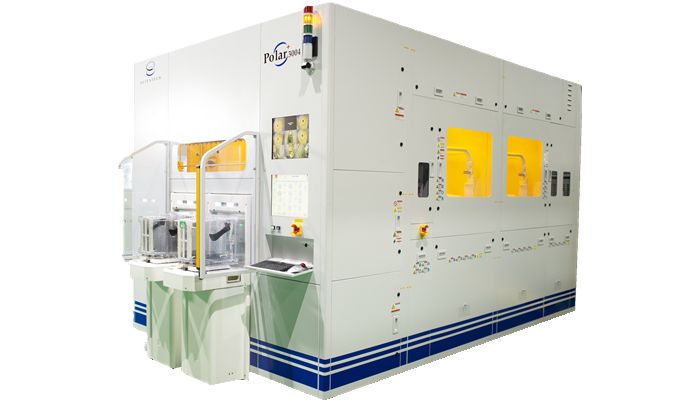
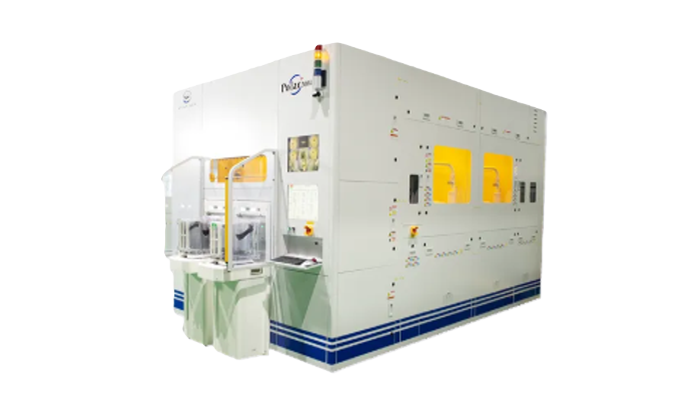
The Polar/Single series represents an advanced system for treating individual semiconductor wafers, widely used in FEOL processes to leverage the output quality. Compared to batch processing methods, single-wafer tools offer notable benefits such as superior process control, customization, decreased contamination risk, and enhanced yield. Single-wafer systems are versatile, can be applied to various applications, and are integrated with features like real-time monitoring, automated handling, and precise control, significantly improving reliability, efficiency, and productivity. These tools play a pivotal role in attaining high-quality semiconductor devices by enabling precise and controlled treatment on individual wafers.
Cleaning | Etching | Stripper |
|---|---|---|
|
|
|
Process | Application | Advantage |
|---|---|---|
|
|
|
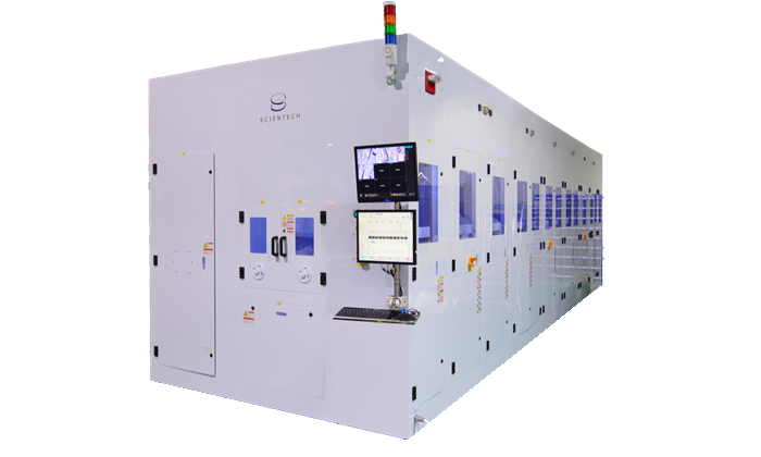
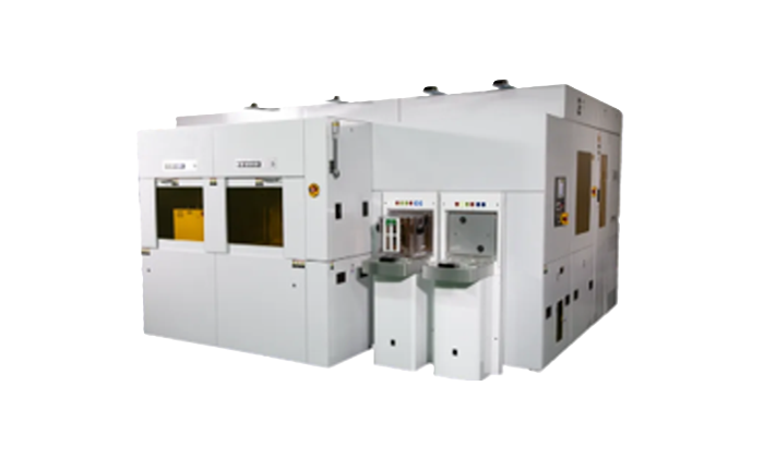
Wet bench systems process multiple wafers simultaneously and are widely used in BEOL processes, including cleaning, etching, and plating. Batch processing offers advantages in terms of throughput and efficiency, making it well-suited for high-volume applications. The equipment optimizes performance by using automated handling, precise chemical delivery, and control systems. Safety measures and waste treatment are integrated to ensure responsible chemical handling. Batch wet processing plays a crucial role in semiconductor manufacturing, enabling efficient and controlled treatment, and resulting in high-quality devices.
Cleaning | Etching | Stripper |
|---|---|---|
|
|
|
Process | Application | Advantage |
|---|---|---|
|
|
|
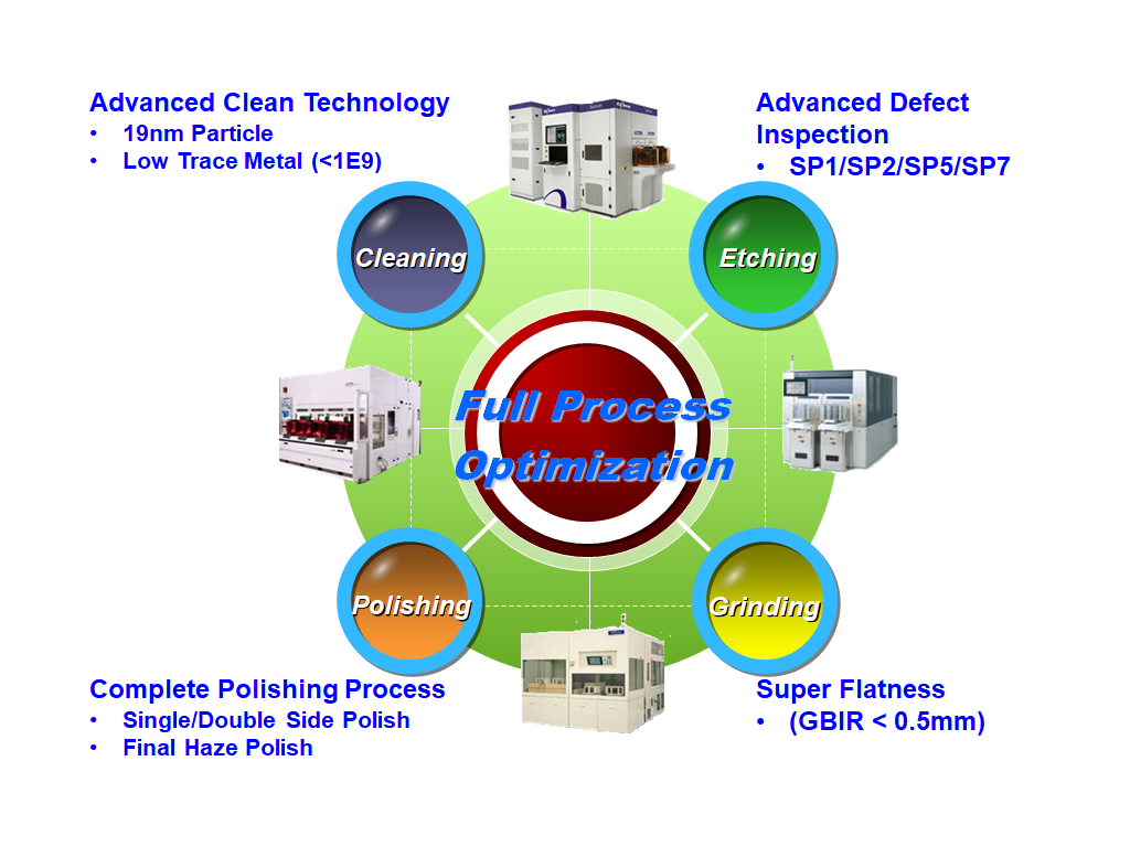
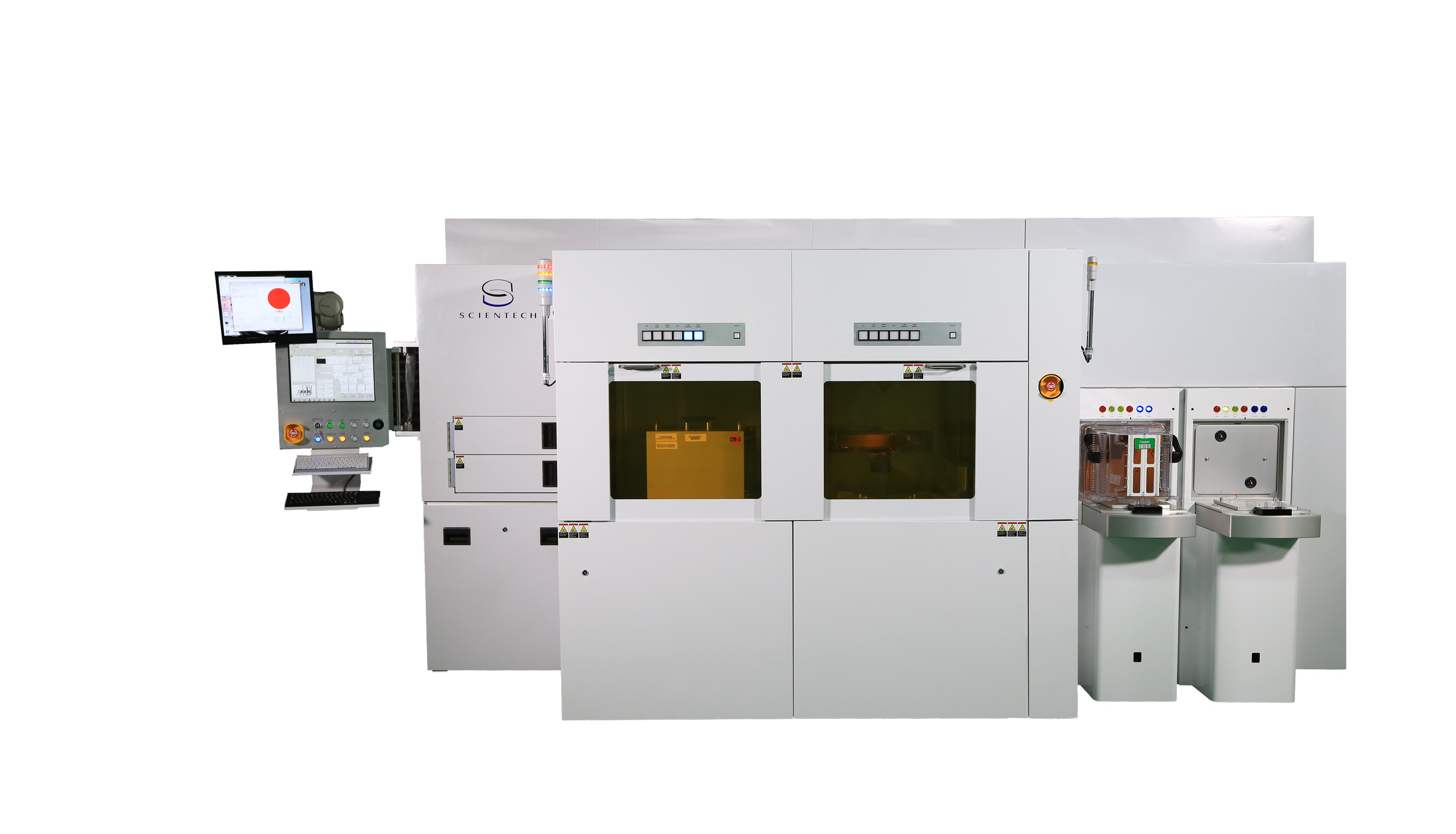
12″ Wafer Reclaim
Copyright © 2026 SCIENTECH. All trademarks and images are the property of their respective owners and protected by law.